Search Result
5 expansions found
Manufacturer C't, Germany | Date 1987 | Amiga A500 | Interface 68000 socket |
- Prozessor Austausch Karte - Processor Exchange Board
- developed by the editors of the german computer magazine c't
- schematics has been fully published in the magazine
- designed to emulate the MC68000 processor bus interface at best, so it can be used in Ataris and Macs as well
- processor
- 68020 @ 12 / 16 MHz, PGA (asynchronous to the motherboard)
- optional 68881 @ 12 / 16 MHz, PGA - runs at the same speed as the CPU
- memory
- optional daughter board with four 32k×8 ROM or SRAM chips
- two boards can be stacked on each other for 256 kB ROM / SRAM total
- notes
- plugs into the 68000's socket
- no 68000 fallback mode

PAK-68 with SRAM module, front side

front side

back side

front side

back side
Manufacturer C't, Germany | Date 1991 | Amiga A500 | Interface 68000 socket |
- successor of the original PAK-68 (Prozessor Austausch Karte - Processor Exchange Board)
- developed by the editors of the german computer magazine c't
- schematics has been fully published in the magazine
- can be used in 68000 based Ataris and Macs as well
- less error prone design - processing flow with state machines
- the discrete logic had been put into GALs, allowing easy reconfiguration in case of timing changes
- the GAL based layout is smaller, making room for ROM/RAM sockets which were located on piggy-back boards on the old board
- processor
- 68020 @ 14 / 16 MHz, PGA
- optional 68881 or 68882 @ 14 / 16 MHz, PGA - runs at the same speed as the CPU
- memory
- four 32 pin sockets for up to 512 kB ROM / SRAM
- when occupied with ROMs, access to OS ROM is 32 bit wide
- SRAMs with 100ns or faster access speed can also be fitted but an additional decoder GAL is necessary
- ROM access can be sped up by 40% by setting a jumper, which disables ROM synchronisation to the 8 MHz clock
- notes
- plugs into the 68000's socket
- either a 68000 has to be put on top of the board or an additional GAL has to be installed
Manufacturer C't, Germany | Date 1994 | Amiga A500 | Interface 68000 socket |
- third generation of the Prozessor Austausch Karte - Processor Exchange Board
- developed by the editors of the german computer magazine c't
- schematics and GAL equations has been fully published in the magazine
- designed to emulate the MC68000 processor bus interface at best, so it can be used in Ataris and Macs as well
- processor
- PAK-68/3-020: 68020
- PAK-68/3-030: 68030
- 14.3 MHz (synchronous) or 32 / 36 / 40 MHz (asynchronous) - could be run in either modes, but requires different GALs
- optional 68881 or 68882 - runs at the same speed as the CPU
- memory
- optional 32 kB level 2 cache
- four EPROM sockets for 32 bit Kickstart access
- memory expansion is possible for the 030 version only
- notes
- the 020 and 030 versions have slightly different layout
- five GALs - there are different GAL sets for each configuration (computer type, CPU type, CPU mode)
- plugs into the 68000's socket
- optional 68000 fallback mode - the 68000 can be installed onto the PAK with an additional GAL

PAK/3-030, back side

PAK/3-030, front side

FRAK30, back side

FRAK30, front side
Manufacturer Great Valley Products, USA | Date 1992 | Amiga A2000, A3000, A4000 | Interface Zorro II | Autoconfig ID 2017 / 11 |
- integrated voice mail and fax system
- Yamaha YTM401 voice-fax chip
- sending and receiving of faxes at 2400-9600 bps
- auto fax detection
- audio record and play back at 9600 Hz, 8 bit
- two RCA connectors: line in for digitizing, line out for audio monitoring of incoming calls
- two RJ11 telephone jacks: one to the phone line, the other to a local telephone
- audio can be recorded and played back through the local telephone too
- an attached fax machine can be used as scanner
- voice compression feature
- record and play back of voice and fax messages remotely
- schedule sending faxes
- multiple PhonePaks can be installed for multiple phone lines
- multiple PhonePaks can share mail boxes
- in order to use the PhonePak in an A3000 or A4000, a Zorro II RAM expansion has to be added in another slot because these machines have problems with Zorro II DMA to Chip RAM

front side

front side
- PhonePak-101.dms
install disk v1.01
578 kB - PhonePak_Messages.dms
messages disk
673 kB - ppak1.dms
GVP-M
install disk 1 v2.4
440 kB - ppak2.dms
GVP-M
install disk 2 v2.4
661 kB - ppak25.dms
GVP-M
v2.5 upgrade
441 kB - ppak3.dms
GVP-M
install disk 3 v2.4
508 kB
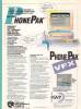
Advert (US)
1992-09
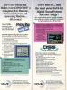
Advert (US)
1992-11
Advert (US)
1993-03
Advert (US)
1993-08
Advert (US)
1993-11
Advert (US)
1994-04
Manufacturer Quikpak / Eagle Computer Products, USA | Date 1997 | Amiga A4000 | Interface CPU slot |
- processor
- 68060 @ 56.75 MHz
- supported processors:
- 68040 @ 40 MHz
- 68060 @ 50 - 66 MHz
- memory
- four 72 pin SIMM sockets accept 128 MB RAM
- supports 4, 8, 16, 32 MB SIMMs
- burst RAM access is supported only if SIMMs are installed in matching pairs
- EDO RAM support (can be disabled) reduces the number of wait states from 2 clocks to 1 clock per 32 bit access
- selectable RAM access speed: 50 or 60 ns for 66 MHz, 60 or 70 ns for 50 MHz, 70 or 80 ns for 40 MHz
- RAM-Cache, based on 10 ns VRAM
- up to 118 MB/s CPU memory access (@ 66MHz)
- up to 20 MB/s DMA memory access
- Kickstart remapping
- optional 32 bit DMA SCSI controller
- the board had to be returned to the manufacturer for installing the required components and the autoboot ROM
- 50 pin internal SCSI header
- hard disk activity connector
- jumper settings
- rev 1 & 2
- rev 3 & 4
| JR1 - | fast memory write: OFF - enabled |
| JR2 - | burst mode: OFF - enabled |
| JR3 - | RAM speed: OFF - faster access time |
| JR4 - | FCLK: ON - >58 MHz |
| JR5 - | EDO RAM support: OFF - enabled |
| JR6 - | RAM size: ON - 16 or 32 MB, OFF - 4 or 8 MB |
| JR7 - | RAM type: ON - double sided, OFF - single sided |
| JR8 - | SCSI: ON - enable |
| JP1 - | reserved |
| JP2 - | cache burst to A4000 motherboard: ON - enabled |
| JP3 - | interrupt pending: ON - DMA backoffs, OFF - DMA ignores interrupt |
| JP4 - | LUN scan: OFF - enabled |
| JP5 - | autoboot: OFF - enabled |
| JP6 - | EPROM type: 1-2 - 27C256, 2-3 - 27C512 |
| JP7 - | CPU power: 1-2 - 5V, 2-3 - 3.3 V |
| JP8 - | CPU clock: 1-2 - 68040, 2-3 - 68060 |
| JP9 - | (rev 2 only) system clock: ON - >60 MHz, OFF - <60 MHz |
| JR1 - | burst mode: OFF - enabled |
| JR2 - | RAM speed: OFF - faster access time |
| JR3 - | reserved |
| JR4 - | reserved |
| JR5 - | RAM size: ON - 16 or 32 MB, OFF - 4 or 8 MB |
| JR6 - | RAM type: ON - double sided, OFF - single sided |
| JR7 - | EDO RAM support: ON - enabled |
| JP8 - | CPU clock: 1-2 - 68040, 2-3 - 68060 |
| JP9 - | CPU power: 1-2 - 5V, 2-3 - 3.3 V |
| JP10 - | EPROM type: 1-2 - 27C256, 2-3 - 27C512 |

front side

back side
- QuickPak060.pdf
User Manual
5.0 MB

Advert (US)
1996-12
Advert (US)
1997-02
Advert (US)
1997-03